
The APS-C-sized sensor in Samsung’s new NX1 uses a BSI sensor. Bob Newman explains what it is
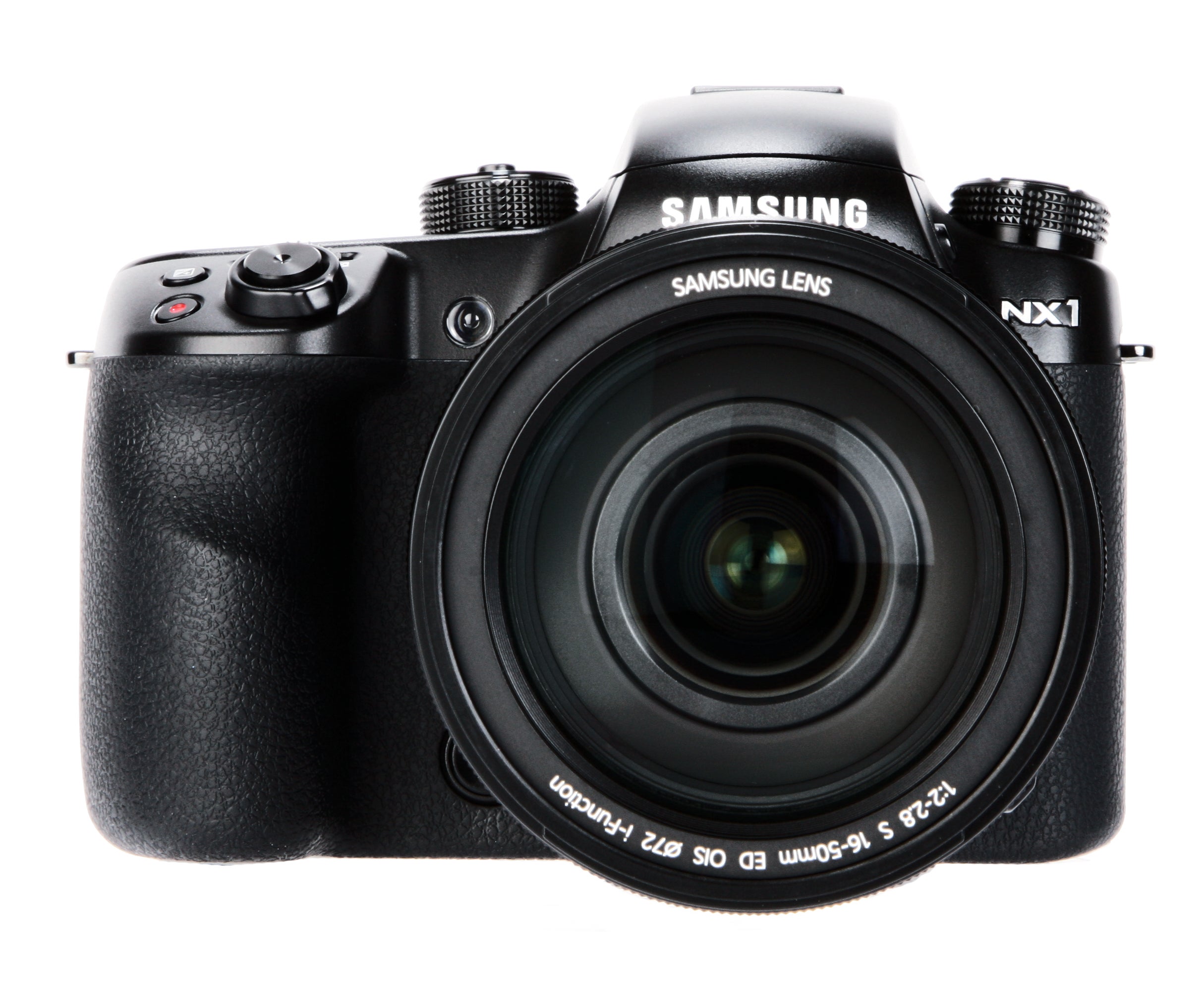
The Samsung NX1 has a 28.2-million-pixel, APS-C BSI sensor
Samsung has not been regarded as one of the great innovators in the world of photography, as it’s a business the company has been involved in for a relatively short time. Back in 2006, Samsung started selling copies of Pentax DSLRs – a relationship that developed with the electronics giant through developing imaging sensors for Pentax. This collaboration seemed to come to an end when Pentax was bought by Hoya, and Samsung went its own way by developing its own range of NX mirrorless interchangeable-lens cameras. These have been competent cameras, perhaps without ‘standout’ features.
Now Samsung has launched the flagship NX1 model, which certainly does have a standout feature – the 28.2-million-pixel, APS-C-sized sensor utilising backside illumination (BSI) technology. This is the first consumer BSI sensor of this size, the previous biggest being the 1in-sized Sony Exmor-R sensor. To understand the progress that Samsung has made, a 1in sensor has approximately one third of the area of an APS-C-sized sensor.
So why is the fitting of a BSI sensor significant? Simply because its efficiency, with respect to collecting photons, is about 50% more than the typical conventional sensor – so fitting a BSI sensor is equivalent to capturing 1⁄2 stop more light, or 1⁄2 stop greater exposure.
The BSI sensor has this greater efficiency because the light impinges directly onto the photoreceptors, rather than having to thread its way through a maze of circuitry as on a conventional sensor. This is achieved by turning the sensor over so that the light is collected by the opposite side of the sensor, hence the term ‘backside illumination’.
A BSI sensor starts out being fabricated in a very similar way to a conventional one. However, once the wafer has been fabricated and the metal wiring applied, the production process diverges. Where a conventional sensor would have the ‘toppings’ (colour filter array and microlens layers) applied at this stage, the BSI wafer is instead bonded to a carrier wafer or ‘handle’. This bonding process is critical, and in the past has failed to produce good yields for large sensors.
Once bonded to the carrier, the wafer is turned over and its back ‘thinned’ or etched away to expose the photodiode backs to the light. Then the toppings are applied to the back side.
A BSI sensor is more expensive than a conventional one for two reasons. First, there are more process steps required, and second, the bonding process can adversely affect the number of good sensors yielded by a wafer.
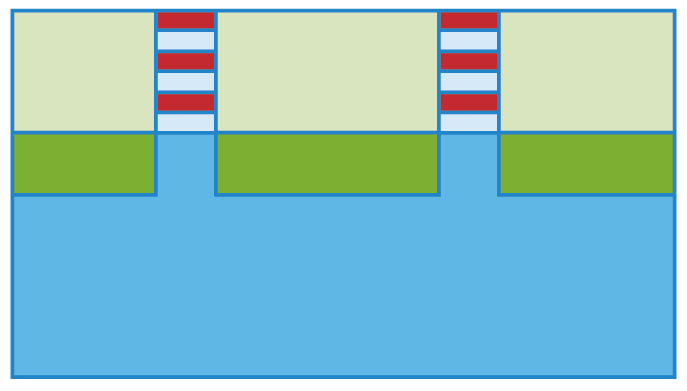
Wafer processed as normal
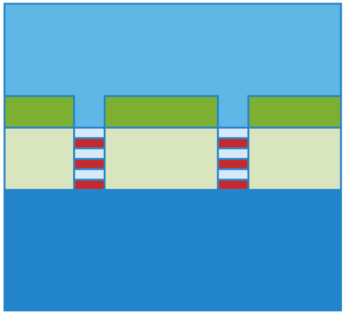
Wafer flipped over and bonded to carrier wafer
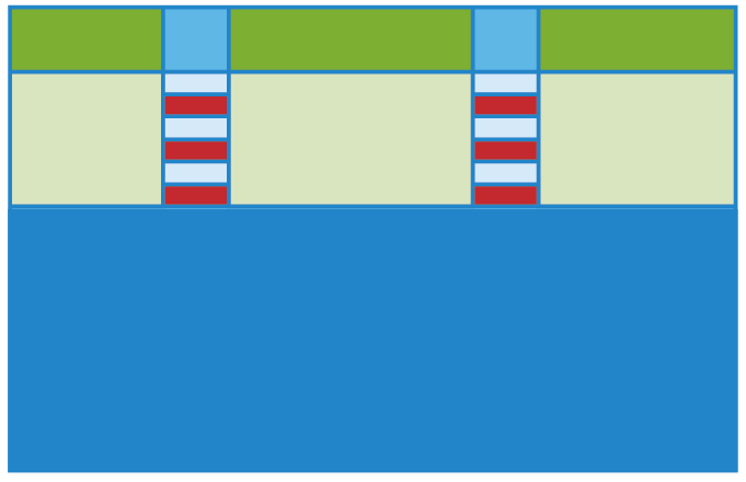
Original wafer thinned to reveal backs of photodiodes
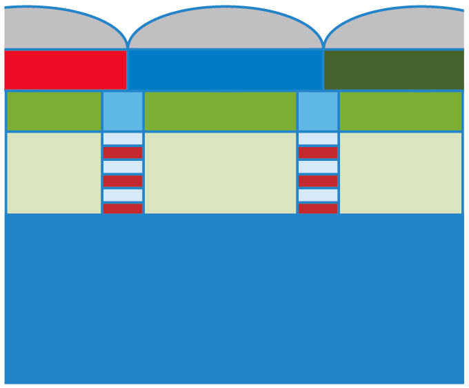
Colour filter array and microlens layers added