
Professor Bob Newman explores the performance-enhancing power of sensors
Some modern sensors retain the colour filters within a metal grid, allowing less leakage between pixels and a shallower ‘optical stack’
The two major manufacturers now seem to follow a four-year release cycle for their top-end cameras. With 2016 an Olympic year, Canon and Nikon have released models aimed at professional photojournalists, in the shape of the EOS-1D X Mark II and D5 respectively. Later, we will see the phased release of lesser products, with the technology in these two cameras trickling down through the range.
This is a time of specification battles, as each company vies to outdo the other in terms of the easily quantifiable metrics of perceived excellence. At this time, nerds like myself are looking beneath the surface, trying to find out how these specification advances have been achieved.
I discovered an interesting document that details some of the more subtle advances that have been taking place in sensor technology, largely unheralded in the present marketing battle, but incrementally increasing the performance of the cameras that we use. The document, by Ray Fontaine, is a summary of some of Chipworks’ discoveries as they dissect different manufacturers’ sensors. You can find it at http://bit.ly/1QKt9Jc. Here I will summarise some of the interesting information from this paper.
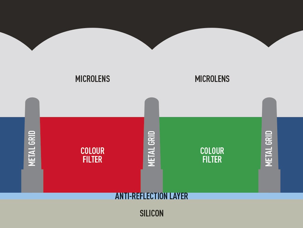
Often small advances can make a difference if applied consistently. Sir David Brailsford, the cycling coach, pursues a philosophy of aggregation of marginal gains with great success. The same philosophy applies to development of products such as image sensors – in general, it isn’t so much revolutions and inventions that bring success, but constant research and development, honing the performance of different parts of the device. One such part is the colour filter array (CFA), which filters the light directed at the pixels of the sensor. Chipworks has discovered that production sensors have moved on from the multicoloured layer of film found on earlier sensors. Now Sony, Panasonic and ON Semiconductor (Aptina) have developed the array into individual filters deposited into a grid arrangement of ‘walls’ between the pixels.
In the Sony and Panasonic examples, the ‘walls’ are made of aluminium, deposited onto the surface of the chip; in the ON Semiconductor example, the square pits are etched into the top layer (the ‘overglass’) of the chip itself. The walls stop light leaking between pixels and also allow a much thinner layer of filter material to be used. This has allowed the total thickness of the optical stack, the CFA and microlenses, to be reduced to 1.5 microns, reducing the focal length of the microlenses, thereby making them faster for better efficiency, especially at the edges of the frame.
Another trend is towards stacked sensors, where the sensor is composed of a stack of chips. The major advantage is that it allows different functions of a modern sensor to be optimised, resulting in potentially higher performance. Sony, Samsung and OmniVision have released stacked sensor chips. In the second-generation Sony devices, the top chip serves solely as a pixel array. All the signal processing, including Sony’s class-leading column analogue-to-digital converters, resides on the lower chip, which uses a different silicon process with smaller geometry than the pixel array, giving faster performance and lower power consumption. The chip also includes data buffers, decoupling the host camera from the timing demands of an unbuffered sensor.
Bob Newman is currently Professor of Computer Science at the University of Wolverhampton. He has been working with the design and development of high-technology equipment for 35 years and two of his products have won innovation awards. Bob is also a camera nut and a keen amateur photographer.